

Gửi bình luận
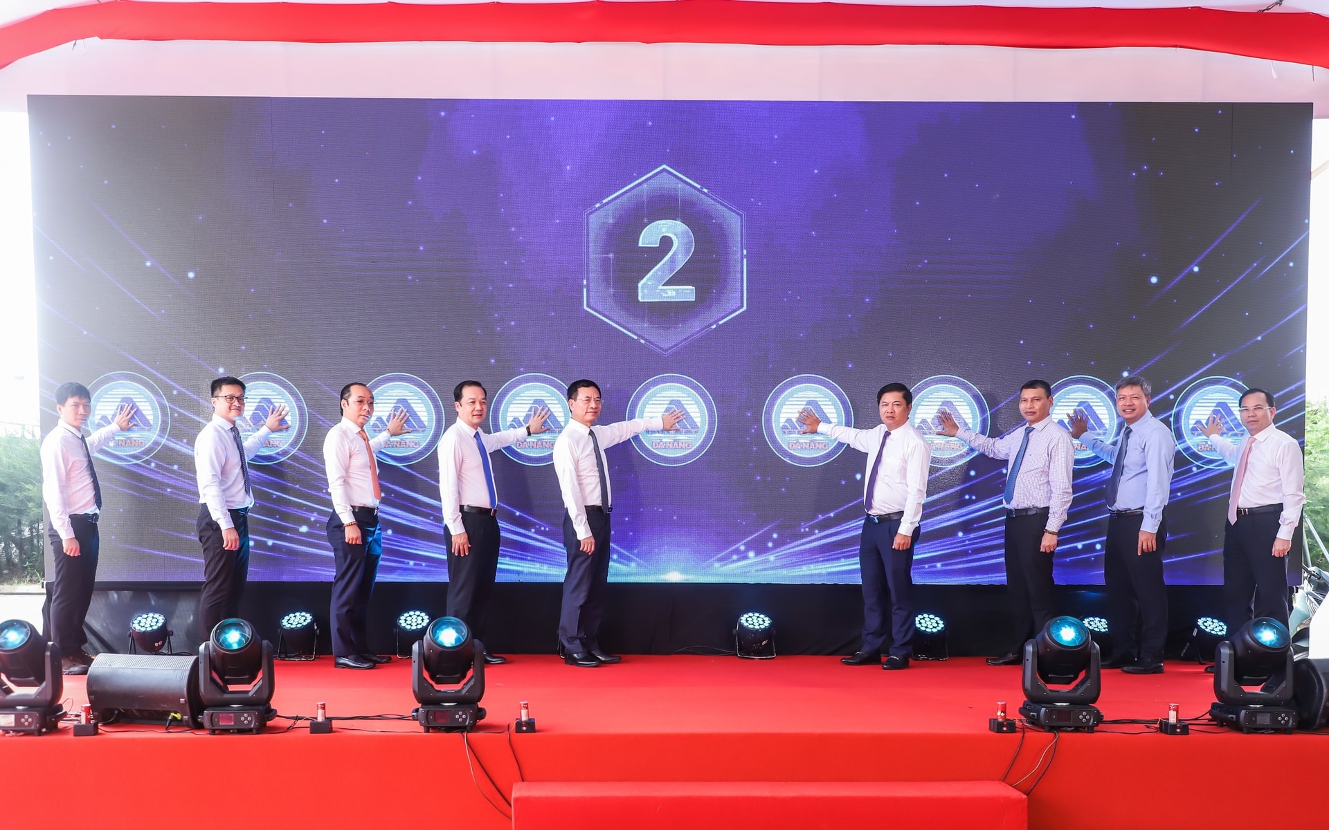
DNO - Work on the Advanced Semiconductor Packaging Laboratory (Fab-Lab) project, located at the Da Nang Software Park No. 2, started on Monday morning.
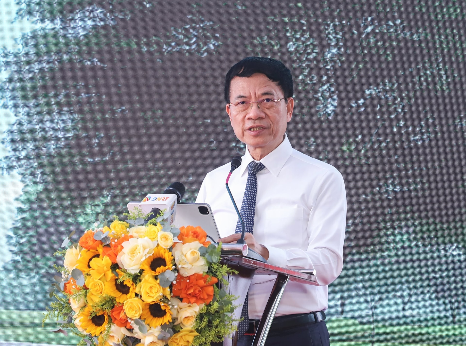
Speaking at the groundbreaking ceremony, Minister of Science and Technology Nguyen Manh Hung highly appreciated the proactive, determined and pioneering spirit of the leaders of Da Nang in creating a favorable environment for the development of the semiconductor industry.
He also emphasized that the launch of the project marked an important milestone in the context that Vietnam is implementing the Party and Government’s major policies on semiconductor industry development.
Minister Hung voiced his hope that VSAP Lab JSC, the project’s developer, will focus on advanced packaging technologies and train highly qualified engineers and experts. This will serve as a launchpad for "Made in Vietnam" technology products and a source of inspiration for the next generation to master core technologies.
He noted each lab like VSAP will be an important piece in building a national semiconductor ecosystem.
He also affirmed that the Ministry of Science and Technology will continue to accompany Da Nang and businesses on this journey by developing incentive mechanisms and investment policies, forming a semiconductor ecosystem in Central Viet Nam, creating favorable conditions for lab models like VSAP to access investment funds, and strengthening international cooperation in chip research, design, packaging, and testing.
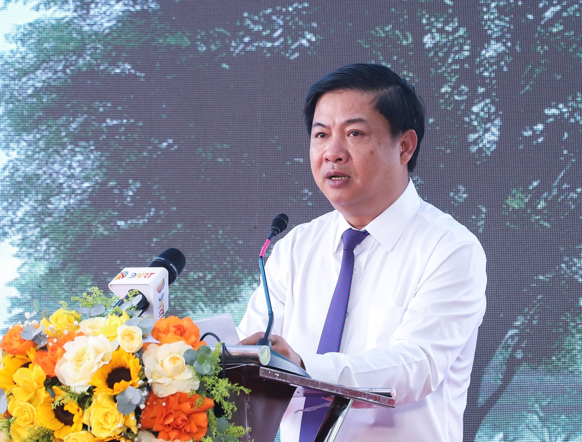
In his remarks at the ceremony, Chairman of the municipal People's Committee Luong Nguyen Minh Triet expected VSAP Lab to be the city's first "Fab-Lab" model that integrates research, testing, pilot production, and hands-on training.
Da Nang is committed to continuing to accompany and support businesses in investing, upgrading and expanding VSAP Lab in a synchronous and modern direction. It will also provide the best possible facilitation in terms of administrative procedures, and auxiliary infrastructure to ensure the project will be completed on schedule.
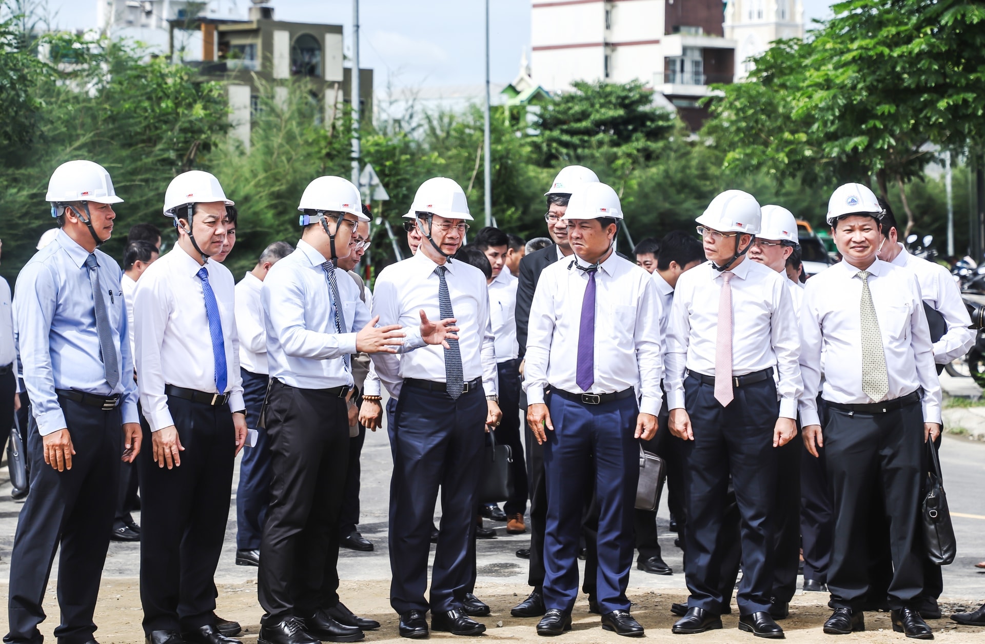
The VND 1.8 trillion project will cover an area of 2,288 square meters, with a total floor area of more than 5,700 square meters. It is expected to be put into operation in the fourth quarter of 2026.
The facility will consist of two main areas: a lab space for research and development of advanced packaging technologies such as Fan-out Wafer Level Packaging (FOWLP), 2.5D/3D IC, silicon interposer, and silicon-bridge; and a fab area for pilot production using real wafers, equipped with cutting-edge systems such as lithography, wafer bonding, and internationally standardized testing and measurement equipment.
Once completed and operational, the facility is expected to reach a design capacity of 10 million units per year to serve both domestic and international markets.